C4Computer Case Climate Controller |
|||||||
|
The "sacreligous" group
|
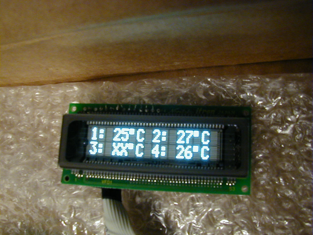
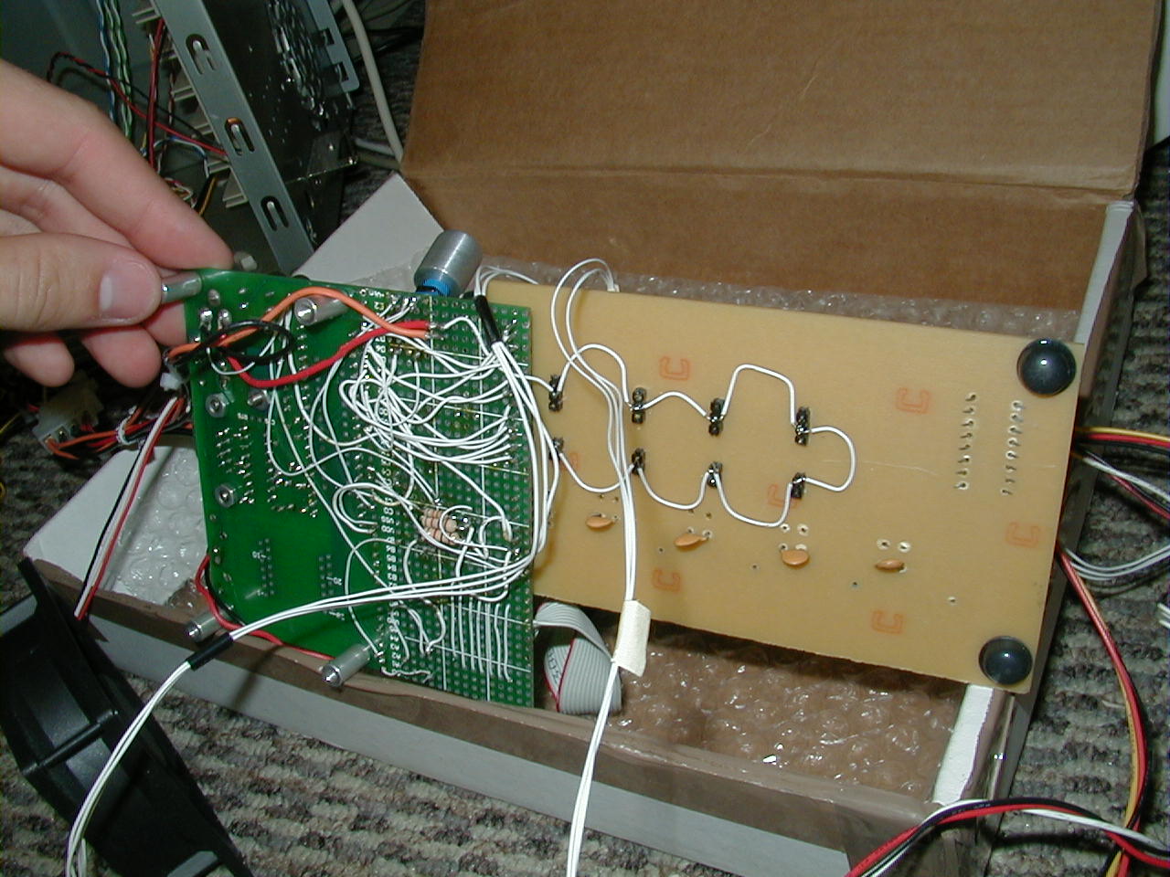
decription:The C4 was a senior design project made by the group "sacreligous" (erik rainey, justin domnitz and stan gryskiewicz III) for ECE4005b taught by John Peatman at the Georgia Institute of Technology in Atlanta, GA, USA. The C4 works by reading the temperature from a series of LM84 remote temperature sensors over an SMBus (really I2C) and then converting those into duty cycle modulations for a series of standard ATX case (3 pin) fans. Currently there are 3 independantly controlled sensor/fan feedback loops. The design can support 4, however one of our LM84 chips was bad. At the center of C4 is the PIC 16F877 microcontroller on a PICLoader board. The PICLoader board is a little hobbist board which has a resident program in a 40 pin PIC 16F877 that allows you to program it over a serial cable. Unfortunately only a Windows compiler exists (to my knowledge) for this chip type.
purpose:The intended purpose of the C4 was control the temperature of a computer case within the abilities of the components while using a minimum of power. There could be some foreseable circumstance where one might need to regulate the power of cooling systems (fans in this case) inorder to fit design specifications, or just because it's neat. components:The following components were used in the deign of the C4:
PDFs for most of these components can be found to the left in the menu bar. challenges:The first challenge was obtaining data sheets from Noritake. On their website is a terse data sheet, which one must register with them to obtain. To obtain a data sheet that contains useful software commands one must request it through a web-interface or by calling a local distributor. They will then fax you a poor visual copy of a full data sheet. This created problems programming the VFD routines as some commands were difficult to read off the data sheet. Creating a somewhat stable feedback loop with a temperature variable was thought to be easy. Since the designers of this project are Computer Engineers, we really had very little training in Controls. We did know that this system would turn into an under-damped response (EE term). After consulting with individuals of other major and more importantly, controls oriented backgrounds it was explained that a perfect control mechanism is almost impossible. To add to this the sensors themselves do not report a steady temperature even in a placid, STP enviroment. This is due to many factor which are not really important. What is important is that the sensors do not report a stable temperature. This factor had to be integrated into the control algorithm.
pictures:All of these images where taken with a digital camera (a nice one too!) and are large, around 240k each. But they are worth it.
PCB HOWTO:Making a PCB board is relatively simple. First you will need to gather the required item necessary to etching a copperboard. These items are, in no particular order:
The last item is the actual layout of the IC's, resistors, caps, etc, on the board. The PCB design for C4 was done using ExpressPCB. The software is easy to learn and use. An interesting point is that it uses milli-inches to express length. Make sure you get the correct pin spacing on all your ICs. The company who makes and distributes the software does so with the mindset that a PCB created with their software will be given to them to create. We did not do so in this case only because of the cost and delay in production. Their website has details on their service if you wish to partake of it. The Express PCB software prevents you from creating etched boards from their software by printing a grayscale background in the design printout. There is no circumvention of this disabling feature, which is why screenshots are used. In the case of the C4, zoomed in screenshots of the final design were taken and pieced together in a graphics package capable of printing exactly to scale. The image in the graphics program was duplicated so that 4 designs would be printed at once on one Press 'n Peel Sheet. It is IMPERATIVE that the design is mirrored horizontally so that it is transfered correctly onto the copperboard. The design was printed. The Press 'n Peel sheet was then cut in half and two designs were placed on one copperboard. At this point the large amount of duplication of designs was done to ensure at least one PCB board would be completed with few errors. The Press 'n Peel material requires ironning to transfer the design from the sheet to the copper board. The instructions say to use a sheet of white paper to buffer the heat between the iron and the Press 'n Peel. The directions indications of time were on the short side. To acheive a nearly perfect transfer we had to iron for about 15 to 20 minutes, moving the iron around every 2 or 3 minutes. Out of 5 transfers 3 were usable. If the transfer did not complete and several traces are broken, the best remedy is to use a fine tipped permanant marker to carefully fill in the broken areas. Be sure to cover over each fixed area several times to make sure that the ink is thick enough to resist etching. Two or three coats is enough. After the design is transferred, the board must be etched. Put on the rubber gloves and carefully pour the etchant into the plastic container you have chosen. Only pour enough to allow the board to float on the surface and have about a 1/4 of liquid under it. BE CAREFUL with etchant. It will stain clothes and I hear it will stain skin but only temporarily. Either way be careful. Now set the board in the etchant and wait for about 20 minutes. If there is a speckling of copper still left just pour a little more etchant in and mix it up. Once the etching is done take the board to a sink (don't get etchant on the rug!) and rise it with cold water. This stops the chemical reaction. Now you will have to drill the holes. Find a drill press you can borrow; don't use a hand drill. This is because of the exacting nature of the holes that need to be drilled. You will need a 60 millainch drill bit. Once you have drilled the board you are ready to solder components on! Happy Hacking!  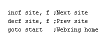 [Skip Prev] [Prev] [Next] [Skip Next] [Random] [Next 5] [List Sites] [Join Ring] this webpage is a production of e.m.rainey
|
||||||